
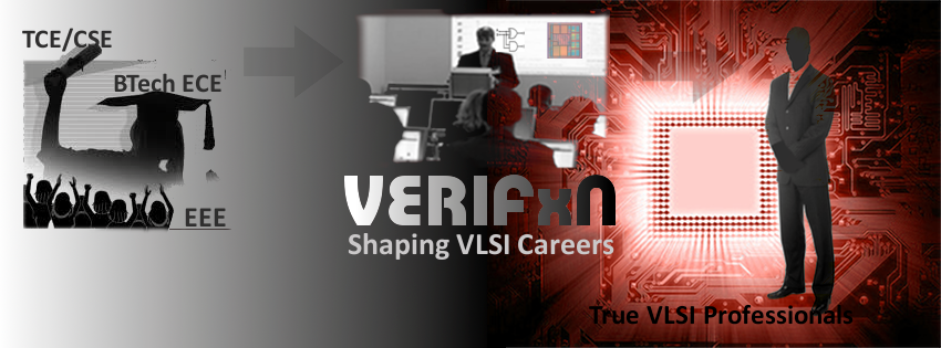
Design Verification (DV) is critical component for successful state-of-the-art Processor, SOC chip design. We (Verifxn) offers training focused on: 1) VLSI Design & Verification * System Verilog, UVM, OVM, VIP, Testbench, IP/SoC/System Level ASIC Verification. * Verilog RTL Coding, Low Power Design, Synthesis, STA, DFT. 2) Hands-on Experience with Industrial Projects. 3) Professional Interview preparation for Semiconductor/Chip Industry jobs.
Sunday, October 20, 2013
Friday, May 24, 2013
How Chips are Built?
A few weeks back a friend of mine asked me if I could quickly explain important steps taken in building the chip - from Marketing idea to final tapeout. Interestingly, I couldn't explain to him very clearly at that moment, nonetheless, that did prompt me to compile related info all at one place.
ASIC Design Flow - Concept to Tapeout
There are about 12 major steps: starting with Marketing requirements to Tapeout when the chip layout database is shipped to chip foundaries like Global, TSMC, UMC.

- Marketing Requirements: Marketing team often researches -- interacting with customers and analyzing competition -- and compiles product specifications like performance goals; cost, power budgets; and schedule.
- Architecture: Chip Architects perform feasibility analysis, and define a higher level architecture that fits marketing specs. The Architecture is then reviewed with Marketing and other stakeholders. If agreed, Architects/Designers develop implementation level plan, often termed as detailed or micro architecture.
- RTL Design: Chip Architects perform feasibility analysis, and define a higher level architecture that fits marketing specs. The Architecture is then reviewed with Marketing and other stakeholders. If agreed, Architects/Designers develop implementation level plan, often termed as detailed or micro architecture.
- RTL to Gates Synthesis: Chip Architects perform feasibility analysis, and define a higher level architecture that fits marketing specs. The Architecture is then reviewed with Marketing and other stakeholders. If agreed, Architects/Designers develop implementation level plan, often termed as detailed or micro architecture.
Sunday, May 19, 2013
Design Verification (DV) Overview
With ever
increasing complexity of state-of-the-art chips, hundreds of millions
gates and billions of transistors, with complex low power states, the
task of verifying that the logic design conforms
to specification is becoming more and more important. The VLSI Industry
pundits are advocating more so for the 3-4 Verification Engineer per
Designer rule, also known as 3-1 rule.
The
Design Verification attempts to answer the question "Does this proposed
design do what is intended?" This is a complex task, and takes the
majority of time and effort in most large Processor, SOC design
projects. More widely viewing the role of DV engineers does not limit to
only functional verification, it includes non-functional aspects like
Low-Power Verification, Timing, Design to Layout Formal equivalence.
Functional
verification is very difficult because of the sheer volume of possible
testcases that exist in even a simple design. For a chip that receives
total 100bits of binary inputs, ideally you will simulate all 2^100 =
2^80 Million possible combinations over those many clock cycles to prove
that, when manufactured, chip is going to work correctly. Presuming you
could simulate 1 million patterns per second you still need 2^80
million seconds to simulate it all, which you dont necessarily have in
our life, to put into perspective there are only 2^31.55 seconds in 100
years.
Such
is the volume of the problem DV engineers deal with. There is lots of
smartness goes into creating a testplan that gives the coverage
comparable to exhaustive input patterns without spending 100s of human
life time to sign off on verification. There is a combination of
techniques applied to conquer the Verif challenge:
- Logic simulation: Simulates the chip before using industry standard simulators like: VCS, ModelSim etc.
- Emulation: Builds a version of system using programmable logic. This is expensive, and still much slower than the real hardware, but orders of magnitude faster than simulation. Example: Quickturn.
- (Semi) Formal verification attempts to prove mathematically that certain requirements (also expressed formally) are met, or that certain undesired behaviors (such as deadlock) cannot occur.
- Intelligent verification uses automation to adapt the testbench to changes in the register transfer level code.
Subscribe to:
Posts (Atom)